) 3K+
3K+
Start Your Learning Journey Today
550+ Students Placed Every Month Be The Next!


Our Hiring Partners
Curriculam Designed By Experts
Expertly designed curriculum for future-ready professionals.
Industry Oriented Curriculum
An exhaustive curriculum designed by our industry experts which will help you to get placed in your dream IT company
-
30+ Case Studies & Projects
-
9+ Engaging Projects
-
10+ Years Of Experience
PCB Design Training Projects
Become a PCB Design Expert With Practical and Engaging Projects.
- Practice essential Tools
- Designed by Industry experts
- Get Real-world Experience
LED Blinking Circuit Board
Design a basic single-layer PCB to build a simple LED blinking module. Learn component placement, trace routing, and power flow understanding. A perfect starter to explore PCB design rules and layout practices.
USB Power Supply Board
Create a 5V regulated USB power supply board with essential components. Understand voltage regulation, connector alignment, and safety clearances. Ideal for learning how to manage power sections on a PCB.
Temperature Sensor Module
Develop a PCB integrating an analog temperature sensor with output mapping. Practice routing, grounding, and sensor placement techniques. This project helps in understanding signal integrity basics.
DC Motor Driver Board
Design a 2-layer PCB using H-bridge driver ICs for motor control. Learn routing techniques for high-current paths and noise reduction.
Arduino-Compatible Microcontroller Board
Create your own development board compatible with Arduino architecture. Work with crystal oscillators, reset circuits, and power regulation.
Power Distribution Board
Develop a multi-voltage power module providing 3.3V, 5V, and 12V outputs. Use regulators, fuses, and thermal considerations for safe operation.
High-Speed Communication Board
Design a PCB using differential pairs and impedance-controlled traces. Focus on signal integrity, trace matching, and noise reduction.
IoT Node Mainboard
Develop a complex multilayer PCB integrating sensors, MCU, and RF modules. Learn component placement, power distribution, and signal routing.
FPGA Control Board
Develop a 4-layer FPGA development PCB with high-density routing. Focus on signal integrity, power planes, and thermal management.
Career Support


Placement Assistance

Exclusive access to ACTE Job portal

Mock Interview Preparation

1 on 1 Career Mentoring Sessions

Career Oriented Sessions

Resume & LinkedIn Profile Building
Key Features

Practical Training

Global Certifications

Flexible Timing

Trainer Support

Study Material

Placement Support

Mock Interviews

Resume Building
Upcoming Batches
What's included

 Free Aptitude and
Technical Skills Training
Free Aptitude and
Technical Skills Training
- Learn basic maths and logical thinking to solve problems easily.
- Understand simple coding and technical concepts step by step.
- Get ready for exams and interviews with regular practice.

 Hands-On Projects
- Work on real-time projects to apply what you learn.
- Build mini apps and tools daily to enhance your coding skills.
- Gain practical experience just like in real jobs.

 AI Powered Self
Interview Practice Portal
AI Powered Self
Interview Practice Portal
- Practice interview questions with instant AI feedback.
- Improve your answers by speaking and reviewing them.
- Build confidence with real-time mock interview sessions.

 Interview Preparation
For Freshers
Interview Preparation
For Freshers
- Practice company-based interview questions.
- Take online assessment tests to crack interviews
- Practice confidently with real-world interview and project-based questions.
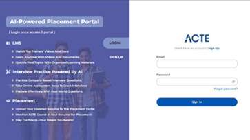
 LMS Online Learning
Platform
LMS Online Learning
Platform
- Explore expert trainer videos and documents to boost your learning.
- Study anytime with on-demand videos and detailed documents.
- Quickly find topics with organized learning materials.
- Learning strategies that are appropriate and tailored to your company's requirements.
- Live projects guided by instructors are a characteristic of the virtual learning environment.
- The curriculum includes of full-day lectures, practical exercises, and case studies.

PCB Design Overview
Benefits Gained from PCB Design Training in Thiruvanmiyur
- Industry-Ready Design Expertise: Students gain a deep understanding of schematic design, layout techniques, signal integrity, and manufacturing considerations, equipping them to handle real-world PCB challenges and meet industry standards.
- Hands-On Tool Experience: Learners work with industry-leading EDA tools to design, test, and optimize PCBs across multiple layers, enhancing their confidence in executing complex projects.
- Better Problem-Solving Skills: The training strengthens analytical thinking, troubleshooting, and design evaluation techniques, enabling students to identify routing issues, EMI problems, and thermal challenges early in the design cycle.
- Strong Career & Industry Exposure: Trainees gain awareness of manufacturing workflows, quality checks, and PCB production processes, expanding job opportunities across electronics manufacturing and design companies.
Emerging Future Trends in PCB Design certification in Thiruvanmiyur
- Rise of HDI & Microvia Designs: High-Density Interconnect PCBs are essential for compact devices like smartphones and wearables. Training includes microvia routing, laser drilling principles, and miniature component placement.
- Integration of AI in PCB Automation: AI-powered layout suggestions and error prediction tools are transforming PCB workflows. Students learn modern automated routing techniques and intelligent placement strategies.
- Growth of Flexible & Rigid-Flex Circuits: Wearables and medical devices increasingly rely on flexible PCBs. Courses cover flex design constraints, bend-radius rules, and reliability testing methods.
- Increasing Use of High-Speed & RF Designs: 5G, EV electronics, and data communication systems require signal-rich boards. Training emphasizes impedance control, RF routing, and antenna integration techniques.
Latest Advancements in PCB Design Course in Thiruvanmiyur
PCB Design Placement in Thiruvanmiyur integrate simulation-driven design to minimize prototype errors. Students gain exposure to high-speed routing techniques and EMI/EMC-aware layout strategies. RF design modules support IoT and wireless devices. HDI methodologies for compact electronics are taught. AI-assisted auto-routing tools improve productivity. Learners practice multilayer stack-ups aligned with industrial standards. Courses cover Gerber generation, vendor coordination, and rigid-flex design. 3D PCB design topics are increasingly emphasized. Low-power PCB techniques promote sustainability. Overall, the curriculum is industry-aligned and practical-focused.
Main Concepts Behind PCB Design certification in Thiruvanmiyur
Placement programs focus on building strong technical fundamentals in PCB layout, schematic design, and electronic principles. Students are trained on real-world design constraints and manufacturing-ready output creation. Mock interviews cover tool proficiency, design logic, and troubleshooting questions. Resume-building sessions highlight projects, skills, and tool expertise. Candidates learn BOM creation, signal integrity, and high-speed routing topics. Effective communication of design decisions is emphasized. Soft skills and teamwork training are included to boost job readiness. Internship opportunities expose learners to real design workflows. Overall, the program ensures students meet industry expectations confidently.
Real-Time Projects Completed Recently in PCB Design Placement in Thiruvanmiyur
Recent projects include multilayer IoT gateway boards, RF sensor modules, automotive-grade motor driver boards, and high-speed communication backplanes. Consumer wearable prototypes with flexible PCBs were delivered. Power management units for solar converters and industrial control boards were completed. Medical diagnostic PCB modules and LED lighting PCB revisions were designed and tested. Smart home automation boards with Wi-Fi connectivity were also developed. PCB Design Course in Thiruvanmiyur hands-on projects helped students secure strong placement opportunities in electronics and PCB design companies.
Career Opportunities After PCB Design Training
PCB Design Engineer
Responsible for schematic creation, PCB layout, routing, DRC checks, and preparing manufacturing files. Works closely with hardware teams to deliver optimized, reliable designs for production.
Hardware Design Engineer
Designs electronics circuits and oversees PCB development meticulously. Ensures boards follow performance, safety, and quality requirements throughout the entire product lifecycle.
Embedded Hardware Engineer
Creates PCB designs for embedded systems, integrating sensors, processors, and communication modules. Focuses on compact, efficient layouts for real-time applications.
Electronics Engineer
Works on product development, testing, and circuit design, including PCB modifications and improvements. Ensures functionality and reliability across electronic components.
DFM Engineer
Ensures PCB designs meet manufacturability standards, reducing production errors and costs. Collaborates with manufacturing teams for smooth transition.
Testing & Validation Engineer
Responsible for testing PCB prototypes, identifying faults, and verifying performance for production readiness. Implements rigorous quality assurance and reliability testing processes.
Skill to Master
Schematic Design
PCB Layout
High-Speed Routing
Signal Integrity Analysis
EMI/EMC Mitigation
Differential Pair Routing
Power Distribution Design
Component Library Creation
Gerber File Generation
DRC/ERC Validation
PCB Simulation
Multilayer Board Design
Tools to Master
Altium Designer
Eagle PCB
KiCad
OrCAD
Mentor Graphics PADS
EasyEDA
Proteus
Cadence Allegro
DipTrace
Multisim
SolidWorks PCB
CircuitMaker
Learn from certified professionals who are currently working.

Training by
Renu, having 12+ yrs of experience
Specialized in: Advanced PCB Layout, High-Speed Design, and HDI Boards.
Note: Renu is recognized for her strong industry expertise, real-time project knowledge, and ability to simplify complex PCB design concepts for learners.
Premium Training at Best Price
Affordable, Quality Training for Freshers to Launch IT Careers & Land Top Placements.
What Makes ACTE Training Different?
Feature
ACTE Technologies
Other Institutes
Affordable Fees
Competitive Pricing With Flexible Payment Options.
Higher Fees With Limited Payment Options.
Industry Experts
Well Experienced Trainer From a Relevant Field With Practical Training
Theoretical Class With Limited Practical
Updated Syllabus
Updated and Industry-relevant Course Curriculum With Hands-on Learning.
Outdated Curriculum With Limited Practical Training.
Hands-on projects
Real-world Projects With Live Case Studies and Collaboration With Companies.
Basic Projects With Limited Real-world Application.
Certification
Industry-recognized Certifications With Global Validity.
Basic Certifications With Limited Recognition.
Placement Support
Strong Placement Support With Tie-ups With Top Companies and Mock Interviews.
Basic Placement Support
Industry Partnerships
Strong Ties With Top Tech Companies for Internships and Placements
No Partnerships, Limited Opportunities
Batch Size
Small Batch Sizes for Personalized Attention.
Large Batch Sizes With Limited Individual Focus.
LMS Features
Lifetime Access Course video Materials in LMS, Online Interview Practice, upload resumes in Placement Portal.
No LMS Features or Perks.
Training Support
Dedicated Mentors, 24/7 Doubt Resolution, and Personalized Guidance.
Limited Mentor Support and No After-hours Assistance.
We are proud to have participated in more than 40,000 career transfers globally.

PCB Design Certification

Real-world experience is helpful but not mandatory for certification. The training itself covers practical design scenarios, industry standards, and tool usage. Freshers can still earn certification by completing course projects and assessments.
Yes, PCB Design Training Course ensure employment. PCB Design Placement Course supports all these aspects to improve your success rate.
Yes, PCB Design Course Certification exam can be taken in Thiruvanmiyur through authorized training centers offering PCB design certifications. Online examination options are also available for added flexibility.
Practical experience is strongly beneficial since PCB design relies heavily on hands-on learning. However, training projects and tool practice can sufficiently prepare beginners for certification exams.
Frequently Asked Questions
- Yes, classroom, online live sessions, and hybrid training formats are available to accommodate different learning preferences.
- Typically ranges from 1 to 3 months depending on the module selection.
- Weekend and fast-track options are also available for working professionals.
- Placement support includes resume preparation, technical interview coaching, mock tests, portfolio building, and direct company drives.
- Yes, the program includes practical PCB projects based on industrial standards and real-world requirements to build hands-on experience.
- Yes, students receive technical interview guidance, HR preparation, mock interviews, and assessment support to enhance placement readiness.