) 3K+
3K+
Start Your Learning Journey Today
550+ Students Placed Every Month Be The Next!


Our Hiring Partners
Curriculum Designed By Experts
Expertly designed curriculum for future-ready professionals.
Industry Oriented Curriculum
An exhaustive curriculum designed by our industry experts which will help you to get placed in your dream IT company
-
30+ Case Studies & Projects
-
9+ Engaging Projects
-
10+ Years Of Experience
PCB Design Training Projects
Become a PCB Design Expert With Practical and Engaging Projects.
- Practice essential Tools
- Designed by Industry experts
- Get Real-world Experience
Battery Level Indicator
This project uses multiple LEDs to show battery levels. It helps beginners grasp voltage division, LED alignment, and layout design for visual outputs.
Simple IR Sensor PCB
Build an infrared-based sensor PCB for object detection. You'll gain knowledge of IR receiver/transmitter placement and signal tracing in a compact layout.
Light-Dependent Switch
Create a PCB that turns on an LED when light levels fall, using LDRs. This helps build skills in analog signal handling and proper orientation of components.
USB Charger Circuit Board
Design a dual-port USB charger with current protection. This project develops skills in USB standards, voltage regulation, and thermal layout
Audio Amplifier Board
Design a small audio amplifier using op-amps or transistors. You’ll focus on signal routing, decoupling, and minimizing noise in audio paths
Capacitive Touch Switch PCB
Create a board that replaces a mechanical switch with a touchpad. You'll learn sensor input circuits, signal smoothing, and insulation planning.
Arduino-Based Home Automation PCB
Build a full home automation PCB with Wi-Fi (ESP8266/ESP32). You'll work on multi-voltage designs, isolation, and communication protocol routing.
GPS Tracker with GSM Module
Design a GPS tracking PCB that sends coordinates via GSM. This complex project teaches power management, antenna placement, and modular design.
Motor Driver Shield for Robotics
Create a dual H-Bridge motor driver PCB compatible with Arduino or Raspberry Pi. You'll focus on current handling, motor control, and thermal dissipation.
Career Support


Placement Assistance

Exclusive access to ACTE Job portal

Mock Interview Preparation

1 on 1 Career Mentoring Sessions

Career Oriented Sessions

Resume & LinkedIn Profile Building
Key Features

Practical Training

Global Certifications

Flexible Timing

Trainer Support

Study Material

Placement Support

Mock Interviews

Resume Building
Upcoming Batches
What's included

 Free Aptitude and
Technical Skills Training
Free Aptitude and
Technical Skills Training
- Learn basic maths and logical thinking to solve problems easily.
- Understand simple coding and technical concepts step by step.
- Get ready for exams and interviews with regular practice.

 Hands-On Projects
- Work on real-time projects to apply what you learn.
- Build mini apps and tools daily to enhance your coding skills.
- Gain practical experience just like in real jobs.

 AI Powered Self
Interview Practice Portal
AI Powered Self
Interview Practice Portal
- Practice interview questions with instant AI feedback.
- Improve your answers by speaking and reviewing them.
- Build confidence with real-time mock interview sessions.

 Interview Preparation
For Freshers
Interview Preparation
For Freshers
- Practice company-based interview questions.
- Take online assessment tests to crack interviews
- Practice confidently with real-world interview and project-based questions.
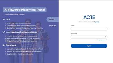
 LMS Online Learning
Platform
LMS Online Learning
Platform
- Explore expert trainer videos and documents to boost your learning.
- Study anytime with on-demand videos and detailed documents.
- Quickly find topics with organized learning materials.
- Learning strategies that are appropriate and tailored to your company's requirements.
- Live projects guided by instructors are a characteristic of the virtual learning environment.
- The curriculum includes of full-day lectures, practical exercises, and case studies.

PCB Design Training Overview
PCB Design Training in Tambaram with Potential Career Paths
A career in PCB Design Program Course in Tambaram opens doors to a variety of high-demand roles in both hardware and embedded systems industries. A PCB Designer can pursue roles such as PCB Layout Engineer, Hardware Design Engineer, Electronics Design Engineer, or Embedded Systems Designer. With the evolution of compact and high-performance electronics, sectors like automotive, aerospace, consumer electronics, and medical devices rely heavily on precise and advanced PCB layouts. As you gain experience, opportunities expand into signal integrity analysis, RF design, and product development leadership roles. Many professionals also find lucrative paths in freelancing, hardware consulting, or entrepreneurship through hardware prototyping and product design startups. PCB designers also collaborate closely with software developers, mechanical engineers, and testing teams, which can lead to cross-functional roles in system integration and electro-mechanical product design.
The Requirements for Learning PCB Design Training in Tambaram
- Basic Electronics Knowledge: To design a PCB effectively, one must have a solid foundation in electronic components such as resistors, capacitors, diodes, and transistors.
- Schematic Diagram Understanding: A key skill for any PCB designer is the ability to read and interpret electrical schematics. Schematics serve as the blueprint for PCB layout, and understanding them is crucial
- Familiarity with CAD Software: PCB design is done using Computer-Aided Design (CAD) tools like Altium Designer, Eagle, KiCad, and OrCAD. Proficiency in these tools enables designers to build, simulate
- Component Datasheet Reading: Designers must be comfortable analyzing datasheets to understand component specifications such as pin configuration, power requirements, and electrical tolerances.
- Digital and Analog Circuit Fundamentals: Understanding the behavior of digital (e.g., microcontrollers, logic gates) and analog (e.g., op-amps, filters) circuits is essential, especially for mixed-signal designs.
Enrolling in PCB Design Certification Course in Tambaram
Enrolling in a PCB Design course equips you with the skills necessary to enter one of the most essential domains in electronics development. From mobile phones to satellites, PCBs form the physical backbone of every electronic device. As the demand for miniaturized and high-performance hardware grows, so does the need for skilled PCB designers. Learning PCB Design empowers you to turn abstract circuit concepts into real, functional boards, and to collaborate effectively with engineers across disciplines. Whether you're a student, hobbyist, or working professional looking to upskill, PCB Design training allows you to innovate in hardware, prototype IoT devices, or even launch your own products. It's also an excellent gateway into embedded systems, automated test design, and hardware troubleshooting.
Techniques and Trends in PCB Design Development Training in Tambaram
- High-Density Interconnect (HDI): HDI technology enables placing more components in a compact area using finer traces, smaller vias (like microvias), and thinner materials.
- Flexible and Rigid-Flex PCBs: These boards combine rigid sections with flexible substrates, offering a hybrid structure that can bend or fold. They're widely used in wearable electronics, aerospace
- Multi-Layer Board Design: Modern electronics often require more than two layers of circuitry, which multi-layer boards provide. By stacking signal, ground, and power planes, these PCBs offer improved signal integrity
- Thermal Management Design: High-performance PCBs generate heat, which can affect performance and lifespan. Techniques like thermal vias, copper pours, and dedicated heat sinks help in efficiently dissipating heat
- Signal Integrity Analysis: As clock speeds and data rates increase, signal distortion, crosstalk, and reflection can disrupt system performance. Signal integrity analysis ensures that electrical signals
The Most Recent PCB Design Coaching in Tambaram with Tool
Modern PCB design Training institute in Tambaram has evolved with powerful and intuitive tools that support everything from simple hobby projects to complex multi-layer industrial boards. Tools like Altium Designer and Cadence Allegro offer extensive features including real-time 3D visualization, advanced simulation, signal integrity analysis, and version control. KiCad and EasyEDA have become increasingly popular among hobbyists and startups for their open-source accessibility and browser-based functionality. Recent trends include cloud-based collaboration, allowing multiple designers to work on a single project in real time, and AI-assisted routing, which improves layout efficiency and minimizes errors. Integration with MCAD tools like Fusion 360 also allows tighter hardware-software coordination, speeding up prototyping cycles. These tools are not just making PCB design faster—they're making it smarter, more accessible, and aligned with next-gen product requirements.
Career Opportunities After PCB Design Training
PCB Design Engineer
A PCB Design Engineer is responsible for creating detailed printed circuit board layouts using CAD tools like Altium Designer, OrCAD, or KiCad. Their tasks include translating schematic diagrams into PCB layouts
Hardware Design Engineer
Hardware Design Engineers design and develop physical electronic circuits and systems, including PCB layouts. They often work closely with embedded system engineers and use PCB design tools to implement
Electronics Design Technician
Electronics Design Technicians assist engineers in developing, testing, and debugging PCB-based electronics. They may work on schematic capture, component selection, and assembling prototypes.
EDA Tool Specialist
An EDA Tool Specialist configures and supports the software used in PCB design, such as Cadence, Mentor Graphics, or Altium. They optimize workflows, troubleshoot tool-related issues, and assist engineering teams
Signal Integrity Engineer
Signal Integrity Engineers analyze and resolve issues related to signal timing, noise, and crosstalk in high-speed circuit boards. Their work ensures that the PCB meets performance standards in environments
DFM Engineer
A DFM Engineer ensures that PCB designs meet manufacturing and assembly standards. They review design files to identify potential issues that may affect fabrication, such as incorrect spacing, pad sizes
Skill to Master
Schematic Capture
PCB Layout Design
Component Library Creation
Signal Integrity Management
Thermal Management Techniques
Design Rule Checking
Gerber File Generation
3D Visualization & Enclosure Fitment
Power Distribution & Ground Planning
DFM
Hardware Debugging & Testing
Collaboration with Cross-Functional Teams
Tools to Master
Altium Designer
Eagle
KiCad
OrCAD
Proteus
EasyEDA
Mentor Graphics PADS
DipTrace
CircuitMaker
Fritzing
LTspice
PCBWay Gerber Viewer
Learn from certified professionals who are currently working.

Training by
Arun, having 7 yrs of experience
Specialized in: PCB Layout Design, Schematic Capture, EMI/EMC Compliance, and High-Speed Board Design.
Note: Arun is well known for guiding engineers through multi-layer board development, especially for medical and automotive applications. His sessions focus on real-time projects using Altium and OrCAD.
Premium Training at Best Price
Affordable, Quality Training for Freshers to Launch IT Careers & Land Top Placements.
What Makes ACTE Training Different?
Feature
ACTE Technologies
Other Institutes
Affordable Fees
Competitive Pricing With Flexible Payment Options.
Higher Fees With Limited Payment Options.
Industry Experts
Well Experienced Trainer From a Relevant Field With Practical Training
Theoretical Class With Limited Practical
Updated Syllabus
Updated and Industry-relevant Course Curriculum With Hands-on Learning.
Outdated Curriculum With Limited Practical Training.
Hands-on projects
Real-world Projects With Live Case Studies and Collaboration With Companies.
Basic Projects With Limited Real-world Application.
Certification
Industry-recognized Certifications With Global Validity.
Basic Certifications With Limited Recognition.
Placement Support
Strong Placement Support With Tie-ups With Top Companies and Mock Interviews.
Basic Placement Support
Industry Partnerships
Strong Ties With Top Tech Companies for Internships and Placements
No Partnerships, Limited Opportunities
Batch Size
Small Batch Sizes for Personalized Attention.
Large Batch Sizes With Limited Individual Focus.
LMS Features
Lifetime Access Course video Materials in LMS, Online Interview Practice, upload resumes in Placement Portal.
No LMS Features or Perks.
Training Support
Dedicated Mentors, 24/7 Doubt Resolution, and Personalized Guidance.
Limited Mentor Support and No After-hours Assistance.
We are proud to have participated in more than 40,000 career transfers globally.

PCB Design Certification

While real-world experience isn’t always a requirement, it significantly enhances your understanding of PCB design principles such as layout optimization and thermal management.
Pursuing a PCB Design certification validates your proficiency in designing printed circuit boards, using CAD tools, and understanding industry-standard practices like EMI shielding, high-speed routing, and thermal control.
Most certifications do not have strict prerequisites, but a basic understanding of electronics, circuit theory, and CAD tools is highly recommended. Familiarity with schematic diagrams, component placement, and layout rules helps you grasp the exam content more effectively.
Yes, ACTE’s PCB Design Certification is worth the time and investment because it offers practical, tool-based training aligned with real industry needs.
Frequently Asked Questions
- Yes, demo sessions are available Before committing to the course, you can attend a demo session to get a clear understanding of the course structure and teaching style.
- Helps in decision-making The demo session allows you to evaluate the course content and trainer’s expertise, helping you make an informed decision.
- ACTE instructors are experienced professionals with significant industry expertise, ensuring that students receive practical and up-to-date knowledge.
- Yes, ACTE provides placement assistance ACTE offers dedicated placement support, including interview preparation, resume building, and job placement referrals to help you secure a job after completing the course.
- Upon completing the PCM Design course, you will receive a certification from ACTE. This certification is recognized by various industries and employers, validating your skills and knowledge in the field of PCB Design.
- Yes, during the PCM Design course, students get the opportunity to work on live projects. This hands-on experience allows you to apply your theoretical knowledge in practical situations, solving real-world problems.