) 3K+
3K+
Start Your Learning Journey Today
550+ Students Placed Every Month Be The Next!


Our Hiring Partners
Curriculum Designed By Experts
Expertly designed curriculum for future-ready professionals.
Industry Oriented Curriculum
An exhaustive curriculum designed by our industry experts which will help you to get placed in your dream IT company
-
30+ Case Studies & Projects
-
9+ Engaging Projects
-
10+ Years Of Experience
PCB Design Training Projects
Become a PCB Design Expert With Practical and Engaging Projects.
- Practice essential Tools
- Designed by Industry experts
- Get Real-world Experience
Basic PCB Design & Schematic Capture
Design a simple single-layer PCB, create the schematic, place components.
Component Library & Footprint Management
Create and manage component libraries and footprints.
Basic Circuit Layout
Multi-Layer PCB Layout
Design a 2–4 layer PCB with optimized component placement and routing. Manage power distribution, signal integrity, and basic EMI considerations.
Power & Signal Optimization
Perform advanced routing, differential pair routing, and ground plane optimization. Analyze performance and prepare design reports.
Prototype PCB Testing
Assemble a prototype PCB, perform continuity and functional tests, identify design errors, and make corrections. Learn real-world troubleshooting techniques.
Complex PCB Integration
Integrate multiple circuits and components into a multi-layer PCB. Ensure signal, power, and thermal integrity across the board.
End-to-End PCB Design Project
Execute a complete PCB project from schematic capture to fabrication-ready files. Perform testing, debugging, and documentation for real-world implementation.
Custom PCB Design & Simulation
Use simulation tools to analyze signal integrity, EMI/EMC, and thermal performance. Optimize the board for reliability and performance.
Career Support


Placement Assistance

Exclusive access to ACTE Job portal

Mock Interview Preparation

1 on 1 Career Mentoring Sessions

Career Oriented Sessions

Resume & LinkedIn Profile Building
Key Features

Practical Training

Global Certifications

Flexible Timing

Trainer Support

Study Material

Placement Support

Mock Interviews

Resume Building
Upcoming Batches
What's included

 Free Aptitude and
Technical Skills Training
Free Aptitude and
Technical Skills Training
- Learn basic maths and logical thinking to solve problems easily.
- Understand simple coding and technical concepts step by step.
- Get ready for exams and interviews with regular practice.

 Hands-On Projects
- Work on real-time projects to apply what you learn.
- Build mini apps and tools daily to enhance your coding skills.
- Gain practical experience just like in real jobs.

 AI Powered Self
Interview Practice Portal
AI Powered Self
Interview Practice Portal
- Practice interview questions with instant AI feedback.
- Improve your answers by speaking and reviewing them.
- Build confidence with real-time mock interview sessions.

 Interview Preparation
For Freshers
Interview Preparation
For Freshers
- Practice company-based interview questions.
- Take online assessment tests to crack interviews
- Practice confidently with real-world interview and project-based questions.
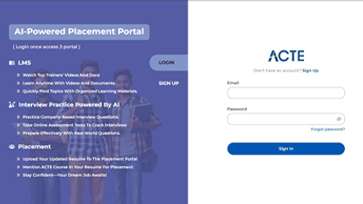
 LMS Online Learning
Platform
LMS Online Learning
Platform
- Explore expert trainer videos and documents to boost your learning.
- Study anytime with on-demand videos and detailed documents.
- Quickly find topics with organized learning materials.
- Learning strategies that are appropriate and tailored to your company's requirements.
- Live projects guided by instructors are a characteristic of the virtual learning environment.
- The curriculum includes of full-day lectures, practical exercises, and case studies.

PCB Design TrainingOverview
PCB Design course in OMR Professional’s Potential Career Paths
PCB design professionals have diverse career opportunities in electronics and hardware design. They can work as PCB Design Engineers, Electronics Design Engineers, Embedded Systems Engineers, or Hardware Consultants in global companies. With expertise in schematic design, PCB layout, and fabrication-ready designs, PCB Design Training with Placement, professionals can handle end-to-end PCB projects, optimize circuits, and support product development. Many also advance to roles in R&D, project management, or hardware system integration.
Requirements for PCB Design certification in OMR
- Basic Electronics Knowledge : Understanding fundamental electronics concepts like circuits, voltage, current, and components is essential for grasping PCB design principles effectively.
- Familiarity with Design Software : Prior exposure to tools like Altium Designer, Eagle, or KiCad helps in navigating PCB software, handling components, and understanding design workflows.
- Computer Skills : Proficiency in Excel, basic CAD operations, and general IT skills is needed for design documentation, reporting, and analysis.
- Analytical Mindset : Strong analytical skills help in interpreting circuit behavior, optimizing layouts, and troubleshooting design errors efficiently.
- Commitment to Learning : Dedication to attending sessions, practicing hands-on exercises, and completing projects ensures successful training completion and readiness for real-world PCB design challenges.
Reasons to Enroll in PCB Design placement in OMR
Enrolling in the PCB Design Training course provides practical experience with real-world circuit design and PCB layout scenarios. Learners gain in-demand PCB design skills for electronics careers. The course is led by industry experts with years of hands-on experience, offering personalized guidance. PCB Design Training Course Students benefit from project-based learning, interactive sessions, and placement assistance with electronics companies. The training ensures readiness for industry certifications and professional implementation.
Techniques and Trends in PCB Design Training
- Hands-On Project Learning : Training focuses on live PCB projects simulating real-world electronics scenarios, providing exposure to end-to-end design cycles and guidance on resolving practical challenges.
- Integration with Electronics Systems : Learn how PCB designs interface with microcontrollers, sensors, and embedded systems for complete product integration.
- Advanced Layout Techniques : Training includes multi-layer routing, high-speed signal integrity, EMI/EMC optimization, and thermal management. Students gain hands-on experience creating optimized, manufacturable boards.
- Real-Time Testing & Debugging : Emphasis on continuity, functional, and in-circuit testing prepares learners for professional environments. Trainees practice fault detection, debugging, and corrective actions.
- Latest Industry Trends : Exposure to modern PCB design tools, fabrication standards, and simulation software ensures learners stay up-to-date with electronics industry best practices.
Modern PCB Design Training Tools
The course leverages tools such as Altium Designer, Eagle, KiCad, PSpice, Gerber Viewers, and CAM software for hands-on practice. Participants use real-time PCB design environments to capture schematics, perform layout, generate fabrication-ready files, and simulate circuits. Advanced features like multi-layer design, PCB Design Course Certifications, signal integrity analysis, and thermal simulations prepare learners for real-world PCB projects. Cloud-based labs and simulation tools enable flexible learning and realistic project experience, ensuring industry-ready skills.
Career Opportunities After PCB Design Training
PCB Design Engineer
Design and implement PCB layouts for electronic circuits. Optimize component placement, routing, and layer stack-ups. Collaborate with engineers to ensure seamless integration with embedded systems.
Electronics Design Engineer
Analyze circuit performance and create optimized PCB schematics. Support product development by simulating circuits, performing signal integrity checks, and refining designs for manufacturing.
Embedded Systems Engineer
Integrate PCB designs with microcontrollers, sensors, and other peripherals. Develop and test complete hardware solutions for IoT, robotics, electronic product and electronic devices.
Hardware Project Manager
Oversee PCB and electronics design projects. Coordinate design, fabrication, and testing workflows. Ensure compliance with quality standards.
PCB Fabrication & Testing Specialist
Manage PCB manufacturing readiness, generate fabrication files, and perform quality inspections. Conduct continuity, functional, and in-circuit testing to ensure reliable boards.
Electronics System Integration Lead
Lead end-to-end PCB projects from schematic capture to assembly and testing. Perform debugging, troubleshooting, and documentation for complex electronic systems.
Skill to Master
Schematic Capture & Circuit Design
PCB Layout Design
Component Placement
Routing & Trace Optimization
Signal Integrity
Power Distribution
Thermal Management
PCB Fabrication File Generation
Design for Manufacturability (DFM)
PCB Testing
Cross-Module Integration
Advanced Simulation
Tools to Master
Altium Designer
Eagle PCB Design Software
KiCad
OrCAD / PSpice
Gerber Viewer & CAM Tools
PCB Layout Simulation Tools
Signal Integrity Analysis Tools
Thermal Analysis Tools
Multimeter & Oscilloscope (for testing)
Soldering & Assembly Workbench
PCB Prototyping Machines (CNC/3D)
Cloud-based PCB Lab & Simulation Platforms
Learn from certified professionals who are currently working.

Training by
Arvind Narayanan, having 12+ years of experience
Specialized in:High-Speed PCB Design, Signal Integrity, and Mixed-Signal Circuits.
Note: Arvind Narayanan is highly regarded for his practical teaching approach in PCB Design Training. He simplifies complex design principles into clear, step-by-step methods, helping learners gain confidence in real-world PCB development.
Premium Training at Best Price
Affordable, Quality Training for Freshers to Launch IT Careers & Land Top Placements.
What Makes ACTE Training Different?
Feature
ACTE Technologies
Other Institutes
Affordable Fees
Competitive Pricing With Flexible Payment Options.
Higher Fees With Limited Payment Options.
Industry Experts
Well Experienced Trainer From a Relevant Field With Practical Training
Theoretical Class With Limited Practical
Updated Syllabus
Updated and Industry-relevant Course Curriculum With Hands-on Learning.
Outdated Curriculum With Limited Practical Training.
Hands-on projects
Real-world Projects With Live Case Studies and Collaboration With Companies.
Basic Projects With Limited Real-world Application.
Certification
Industry-recognized Certifications With Global Validity.
Basic Certifications With Limited Recognition.
Placement Support
Strong Placement Support With Tie-ups With Top Companies and Mock Interviews.
Basic Placement Support
Industry Partnerships
Strong Ties With Top Tech Companies for Internships and Placements
No Partnerships, Limited Opportunities
Batch Size
Small Batch Sizes for Personalized Attention.
Large Batch Sizes With Limited Individual Focus.
LMS Features
Lifetime Access Course video Materials in LMS, Online Interview Practice, upload resumes in Placement Portal.
No LMS Features or Perks.
Training Support
Dedicated Mentors, 24/7 Doubt Resolution, and Personalized Guidance.
Limited Mentor Support and No After-hours Assistance.
We are proud to have participated in more than 40,000 career transfers globally.

PCB Design Certification

Yes, PCB Design certifications are available at various levels. Beginners can start with Associate-level PCB Design Certification, while advanced learners may pursue Professional or Specialist certifications in areas such as High-Density Interconnect (HDI), RF PCB Design, or Advanced Multilayer Boards. These certifications allow learners to build domain expertise and strengthen employability in electronics and hardware industries.
Yes, many professionals pursue multiple certifications to enhance their skill set in PCB Design Course Certifications. For example, combining basic PCB design certification with advanced high-speed board design or RF PCB specialization makes you more versatile. This multi-skill approach increases your career options in both design and manufacturing industries.
Yes, most PCB Design certification exams can be taken online through authorized portals. You can register, PCB Design Training Course, schedule, and attempt the exam remotely. Online options offer convenience for working professionals while ensuring standardized evaluation of PCB design knowledge.
While prior industry exposure helps, it is not mandatory. PCB Design Training programs in OMR provide hands-on projects, simulation practices, and real-world case studies to bridge the gap PCB Design Training with Placement. This ensures learners are placement-ready even without prior experience. Internships and guided projects further prepare students for industry roles.
Frequently Asked Questions
- Yes, PCB Design Certification in OMR is widely accepted in electronics and manufacturing industries. While it complements global certifications, it highlights hands-on expertise and tool proficiency, which recruiters highly value.
- Yes, placement assistance is provided, including:
- Resume preparation for PCB Design roles.
- Technical interview guidance and mock interview practice.
- Job referrals through partnerships with electronics companies.
- Absolutely! The course includes workshops and live design projects covering schematic design, PCB layout, EMI/EMC considerations, fabrication guidelines, PCB Design Training with Placement and design for manufacturing. Learners gain practical experience by working on real-time industry-level projects.
- PCB Design trainers are experienced professionals with 10–15 years of expertise in circuit and board design.
- Many have worked on industrial projects for automotive, PCB Design Training Course, IoT, and telecom products, bringing practical knowledge to the classroom.
- You can register through the training institute’s website or contact their team for a free demo. Demo sessions include an overview of the PCB Design course, PCB Design Course Certifications trainer introduction, and a preview of teaching methods and tools like Altium Designer, OrCAD, and KiCad.