) 3K+
3K+
Start Your Learning Journey Today
550+ Students Placed Every Month Be The Next!


Our Hiring Partners
Curriculum Designed By Experts
Expertly designed curriculum for future-ready professionals.
Industry Oriented Curriculum
An exhaustive curriculum designed by our industry experts which will help you to get placed in your dream IT company
-
30+ Case Studies & Projects
-
9+ Engaging Projects
-
10+ Years Of Experience
PCB Design Training Projects
Become a PCB Design Expert With Practical and Engaging Projects.
- Practice essential Tools
- Designed by Industry experts
- Get Real-world Experience
Basic LED Circuit Board
This project focuses on designing a simple single-layer PCB to blink one or more LEDs using a basic resistor-LED circuit, possibly driven by a 555 timer or microcontroller output.
Simple Power Supply PCB
The goal here is to design a regulated DC power supply circuit on a PCB, commonly converting AC to 5V or 3.3V DC using components like a transformer, bridge rectifier, voltage regulator (e.g., LM7805), and filtering capacitors.
Custom Component Libraries
This project entails building custom schematic symbols and footprints for frequently used or unavailable components in KiCad, Eagle, or Altium.
Microcontroller Interface Board
This project involves creating a PCB to interface popular microcontrollers like Arduino, ESP32, or STM32 with external sensors or modules (e.g., I2C devices, buttons, LCDs).
Signal Simulation Test Bench
In this project, you simulate analog or digital circuits (like amplifiers, filters, or oscillators) before fabricating the PCB.
Gerber File Checker
Develop or use scripts/tools (e.g., Python-based or with open-source utilities) to validate Gerber files and drill files for manufacturing readiness.
IoT Multi-Layer PCB Design
This project involves designing a compact 4-layer PCB for an IoT device that integrates sensors, wireless communication modules (like Wi-Fi or BLE), and a microcontroller.
High-Speed Trace Optimization Tool
Build a utility or plugin (possibly using Python or C++) to help PCB designers automatically manage or validate high-speed trace parameters like length matching, differential pair spacing, and impedance control.
EMI/EMC-Optimized PCB
This project is focused on designing a PCB layout that minimizes electromagnetic interference (EMI) and ensures electromagnetic compatibility (EMC) for compliance with industrial standards.
Career Support


Placement Assistance

Exclusive access to ACTE Job portal

Mock Interview Preparation

1 on 1 Career Mentoring Sessions

Career Oriented Sessions

Resume & LinkedIn Profile Building
Key Features

Practical Training

Global Certifications

Flexible Timing

Trainer Support

Study Material

Placement Support

Mock Interviews

Resume Building
Upcoming Batches
What's included

 Free Aptitude and
Technical Skills Training
Free Aptitude and
Technical Skills Training
- Learn basic maths and logical thinking to solve problems easily.
- Understand simple coding and technical concepts step by step.
- Get ready for exams and interviews with regular practice.

 Hands-On Projects
- Work on real-time projects to apply what you learn.
- Build mini apps and tools daily to enhance your coding skills.
- Gain practical experience just like in real jobs.

 AI Powered Self
Interview Practice Portal
AI Powered Self
Interview Practice Portal
- Practice interview questions with instant AI feedback.
- Improve your answers by speaking and reviewing them.
- Build confidence with real-time mock interview sessions.

 Interview Preparation
For Freshers
Interview Preparation
For Freshers
- Practice company-based interview questions.
- Take online assessment tests to crack interviews
- Practice confidently with real-world interview and project-based questions.
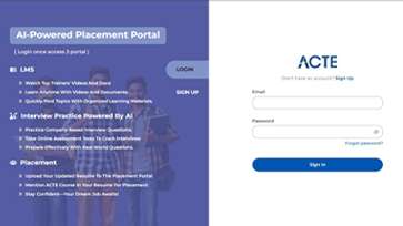
 LMS Online Learning
Platform
LMS Online Learning
Platform
- Explore expert trainer videos and documents to boost your learning.
- Study anytime with on-demand videos and detailed documents.
- Quickly find topics with organized learning materials.
- Learning strategies that are appropriate and tailored to your company's requirements.
- Live projects guided by instructors are a characteristic of the virtual learning environment.
- The curriculum includes of full-day lectures, practical exercises, and case studies.

PCB Design Training Overview
PCB Design Course in Siruseri with Potential Career Paths
Skilled PCB designers are in great demand across multiple industries as the world shifts toward more compact and efficient electronic products. Professionals in this field can take up roles such as PCB Layout Engineer, Embedded Hardware Developer, or Electronics Design Engineer. They play a vital role in developing hardware solutions that power devices in consumer electronics, automotive systems, aerospace equipment, and medical technology. With the rapid growth of IoT and wearable devices, PCB design has become even more critical. Companies value designers who can ensure signal integrity, power efficiency, and manufacturability in their boards. Careers in this domain offer excellent opportunities for innovation and problem-solving. In addition, global demand for electronics ensures steady growth and job security for PCB professionals. For learners, this field opens a path toward both technical specialization and leadership roles in hardware development.
Prerequisites for PCB Design Certification Training in Siruseri
A strong background in electronics, electrical engineering, or embedded systems provides a solid foundation for PCB design training. Learners should have a basic understanding of circuit theory to easily grasp how current, voltage, and resistance interact in circuits. Familiarity with electronic components such as resistors, capacitors, diodes, and ICs helps in working with schematic capture tools. Knowledge of reading and interpreting circuit diagrams gives an added advantage. Computer literacy and comfort with CAD or design software will make learning faster and more effective. While prior exposure to PCB tools is not mandatory, it is helpful for advanced topics. Problem-solving skills and attention to detail are also valuable, as PCB design requires precision. With these prerequisites, learners will be better equipped to successfully transition into hands-on PCB projects and industry roles.
Why Train in PCB Design with Placement in Siruseri
- Strategic Location: Being situated in a major tech hub provides students with exposure to a professional environment from the start. Learners benefit from proximity to top electronics, IT, and R&D companies, which enhances networking opportunities.
- Tool-Based Learning: The program emphasizes hands-on learning with globally recognized EDA (Electronic Design Automation) tools. Students get the chance to design and simulate PCBs using industry-standard platforms such as Altium Designer, Eagle, OrCAD, and KiCad.
- Practical Experience: Theory is complemented by practical exposure to PCB design, prototyping, and fabrication. Students don’t just create virtual designs but also translate them into physical boards, understanding the end-to-end process.
- Industry-Focused Curriculum: The training goes beyond basics and covers advanced concepts needed in modern electronics. Design for Manufacturability (DFM) ensures students learn how to create designs that can be efficiently produced at scale.
- Placement-Oriented Training: The program is structured to bridge the gap between training and employment. Learners get guided support for industry-grade projects that strengthen their portfolio. Resume-building, interview preparation, and mock sessions are part of the placement module.
- Expert Trainers: Faculty members come with years of practical experience in PCB design, testing, and manufacturing. Their expertise brings in-depth insights into current industry trends and challenges.
Modern Trends and Techniques in PCB Design with Placement
The PCB design training in Siruseri is designed to prepare learners for cutting-edge electronics and embedded system development. Courses delve into multi-layer board design, high-speed signal layout, and thermal and EMI/EMC considerations, all of which are critical for designing boards used in automotive, aerospace, and IoT applications. Learners work on design-for-manufacturability (DFM), design-for-testability (DFT), and use simulation tools to test signal integrity before fabrication. Tools like Altium Designer, KiCad, and OrCAD are taught in depth, along with Gerber file generation and Bill of Materials (BOM) creation. Additionally, learners explore rigid-flex board design, HDI layouts, and real-time debugging techniques, ensuring they’re ready for both prototyping and mass production environments.
Latest Tools in PCB Design Certification Training in Siruseri
- Altium Designer & Eagle: Altium Designer and Autodesk Eagle are among the most widely used PCB design tools in the electronics industry. Altium offers a complete environment for schematic capture, PCB layout, component management, high-speed routing, and 3D visualization, making it a preferred choice for professional engineers.
- KiCad & OrCAD: KiCad is a powerful open-source tool that supports schematic capture, PCB layout, multi-layer design, and 3D rendering. Its free availability makes it an excellent choice for students, startups, and research projects.
- Gerber File Generation & DFM Checks: One of the most important steps in PCB design is generating Gerber files, the universal format used by PCB manufacturers. These files include details such as copper layers, solder masks, and drill information that guide the fabrication process.
- Signal Integrity & Power Integrity Analysis Tools: In modern electronics, especially in high-speed and high-frequency designs, ensuring reliable performance requires attention to signal integrity (SI) and power integrity (PI). SI tools help designers identify issues like impedance mismatches, crosstalk, and signal reflections that can disrupt communication in high-speed circuits.
- Simulation Tools for validating electronic circuit designs: Before fabricating a PCB, it is vital to test how the circuit will behave under real-world conditions. Simulation tools, often SPICE-based, allow designers to validate both analog and digital circuits virtually.
- 3D PCB Visualization and Export Tools: Modern PCB design tools include advanced 3D visualization features that allow engineers to inspect the layout in three dimensions before production.
Career Opportunities After PCB Design Training
PCB Design Engineer
Designs and tests printed circuit boards for electronic products.
EDA Tool Specialist
Works with PCB design tools for layout and circuit simulation.
Embedded Hardware Engineer
Develops PCB hardware integrated with embedded systems.
Electronics Design Engineer
Designs electronic circuits and PCB prototypes.
R&D Technician
Assists in prototyping and PCB assembly.
DFM Engineer
A DFM Engineer ensures that PCB designs meet manufacturing and assembly standards. They review design files to identify potential issues that may affect fabrication, such as incorrect spacing, pad sizes
Skill to Master
Schematic Diagram Design
PCB Layout & Routing
Signal Integrity & EMI Considerations
Soldering Techniques (Through-Hole & SMD)
Layer Stack-Up Design
Design Rule Checking (DRC)
BOM & Gerber File Generation
Prototyping & Testing
Power Distribution & Grounding Techniques
Thermal Management in PCB Design
High-Speed Design Principles
PCB Design for Manufacturability (DFM)
Tools to Master
Altium Designer
Eagle PCB
OrCAD
KiCAD
Proteus Design Suite
Multisim
EasyEDA
DipTrace
LTspice
PADS PCB (by Mentor Graphics)
CircuitMaker
Fusion 360 Electronics
Learn from certified professionals who are currently working.

Training by
Arun, having 8+ yrs of experience
Specialized in: Schematic Design and BOM Generation, Multi-layer PCB Design & Thermal Analysis, Component Footprint Creation, High-Speed, Routing Techniques, Design Rule Checking and Validation,PCB Assembly & Testing Support
Note:Priya’s PCB Design course blends foundational circuit knowledge with real-world design tools used in the electronics industry. The program is ideal for electronics engineers aiming to work in embedded systems, hardware design, or product development roles.
Premium Training at Best Price
Affordable, Quality Training for Freshers to Launch IT Careers & Land Top Placements.
What Makes ACTE Training Different?
Feature
ACTE Technologies
Other Institutes
Affordable Fees
Competitive Pricing With Flexible Payment Options.
Higher Fees With Limited Payment Options.
Industry Experts
Well Experienced Trainer From a Relevant Field With Practical Training
Theoretical Class With Limited Practical
Updated Syllabus
Updated and Industry-relevant Course Curriculum With Hands-on Learning.
Outdated Curriculum With Limited Practical Training.
Hands-on projects
Real-world Projects With Live Case Studies and Collaboration With Companies.
Basic Projects With Limited Real-world Application.
Certification
Industry-recognized Certifications With Global Validity.
Basic Certifications With Limited Recognition.
Placement Support
Strong Placement Support With Tie-ups With Top Companies and Mock Interviews.
Basic Placement Support
Industry Partnerships
Strong Ties With Top Tech Companies for Internships and Placements
No Partnerships, Limited Opportunities
Batch Size
Small Batch Sizes for Personalized Attention.
Large Batch Sizes With Limited Individual Focus.
LMS Features
Lifetime Access Course video Materials in LMS, Online Interview Practice, upload resumes in Placement Portal.
No LMS Features or Perks.
Training Support
Dedicated Mentors, 24/7 Doubt Resolution, and Personalized Guidance.
Limited Mentor Support and No After-hours Assistance.
We are proud to have participated in more than 40,000 career transfers globally.

PCB Design Certification

While real-world experience isn’t always a requirement, it significantly enhances your understanding of PCB design principles such as layout optimization and thermal management.
Pursuing a PCB Design certification validates your proficiency in designing printed circuit boards, using CAD tools, and understanding industry-standard practices like EMI shielding, high-speed routing, and thermal control.
Most certifications do not have strict prerequisites, but a basic understanding of electronics, circuit theory, and CAD tools is highly recommended. Familiarity with schematic diagrams, component placement, and layout rules helps you grasp the exam content more effectively.
Yes, ACTE’s PCB Design Certification is worth the time and investment because it offers practical, tool-based training aligned with real industry needs.
Frequently Asked Questions
- Yes, demo sessions are available Before committing to the course, you can attend a demo session to get a clear understanding of the course structure and teaching style.
- Helps in decision-making The demo session allows you to evaluate the course content and trainer’s expertise, helping you make an informed decision.
- ACTE instructors are experienced professionals with significant industry expertise, ensuring that students receive practical and up-to-date knowledge.
- Yes, ACTE provides placement assistance ACTE offers dedicated placement support, including interview preparation, resume building, and job placement referrals to help you secure a job after completing the course.
- Upon completing the PCM Design course, you will receive a certification from ACTE. This certification is recognized by various industries and employers, validating your skills and knowledge in the field of PCB Design.
- Yes, during the PCM Design course, students get the opportunity to work on live projects. This hands-on experience allows you to apply your theoretical knowledge in practical situations, solving real-world problems.