
550+ Students Placed Every Month Be The Next!





























Our Hiring Partners

Curriculum Designed By Experts
Expertly designed curriculum for future-ready professionals.
Industry Oriented Curriculum
An exhaustive curriculum designed by our industry experts which will help you to get placed in your dream IT company
-
30+ Case Studies & Projects
-
9+ Engaging Projects
-
10+ Years Of Experience
PCB Design Training Projects
Become a PCB Design Expert With Practical and Engaging Projects.
- Practice essential Tools
- Designed by Industry experts
- Get Real-world Experience
PCB Layout
Design a printed circuit board layout to manage electronic components, circuit connections, trace routing, and board dimensions while applying design rules, validations, and layout optimization.
Circuit Simulation
Perform electronic circuit simulations to evaluate signal performance, voltage levels, and component functionality while implementing electrical verification techniques and circuit analysis methods.
PCB Fabrication
Develop PCB manufacturing files to manage Gerber outputs, drilling specifications, component placement, and fabrication documentation using design verification and validation.
PCB Layout
Design a printed circuit board layout to manage electronic components, circuit connections, trace routing, and board dimensions while applying design rules, validations, and layout optimization.
Circuit Simulation
Perform electronic circuit simulations to evaluate signal performance, voltage levels, and component functionality while implementing electrical verification techniques and circuit analysis methods.
PCB Fabrication
Develop PCB manufacturing files to manage Gerber outputs, drilling specifications, component placement, and fabrication documentation using design verification and validation.
Layer Configuration
Configure PCB copper layers, stackup structures, trace clearances, and routing parameters to improve circuit performance and signal integrity while following design standards.
Routing Optimization
Develop a PCB routing solution to optimize signal paths, minimize interference, manage trace widths, and improve circuit reliability using routing techniques, simulations, and verification.
Gerber Generation
Prepare and generate PCB fabrication files by exporting Gerber layouts, validating drill information, resolving design errors, and verifying manufacturing accuracy using CAD tools.
Career Support


Placement Assistance

Exclusive access to ACTE Job portal

Mock Interview Preparation

1 on 1 Career Mentoring Sessions

Career Oriented Sessions

Resume & LinkedIn Profile Building
Key Features

Practical Training

Global Certifications

Flexible Timing

Trainer Support

Study Material

Placement Support

Mock Interviews

Resume Building
Upcoming Batches
What's included

 Free Aptitude and
Technical Skills Training
- Learn basic maths and logical thinking to solve problems easily.
- Understand simple coding and technical concepts step by step.
- Get ready for exams and interviews with regular practice.

 Hands-On Projects
- Work on real-time projects to apply what you learn.
- Build mini apps and tools daily to enhance your coding skills.
- Gain practical experience just like in real jobs.

 AI Powered Self
Interview Practice Portal
- Practice interview questions with instant AI feedback.
- Improve your answers by speaking and reviewing them.
- Build confidence with real-time mock interview sessions.

 Interview Preparation
For Freshers
- Practice company-based interview questions.
- Take online assessment tests to crack interviews
- Practice confidently with real-world interview and project-based questions.

 LMS Online Learning
Platform
- Explore expert trainer videos and documents to boost your learning.
- Study anytime with on-demand videos and detailed documents.
- Quickly find topics with organized learning materials.
- Learning strategies that are appropriate and tailored to your company's requirements.
- Live projects guided by instructors are a characteristic of the virtual learning environment.
- The curriculum includes of full-day lectures, practical exercises, and case studies.

PCB Design Training Overview
Gain Electronics Design Knowledge with PCB Design Training in Adyar
Electronics industries increasingly depend on reliable circuit boards, accurate component layouts, and efficient design processes to support modern electronic devices. Through structured practical training, learners discover how PCB Design techniques support circuit development, component integration, signal transmission, hardware testing, and electronic product manufacturing. The PCB Design Internship Course In Adyar introduces essential electronics concepts, schematic capture, circuit layout, component placement, trace routing, multilayer PCB design, design rule checking, signal integrity, and manufacturing documentation using industry-relevant tools such as Altium Designer, KiCad, OrCAD, Autodesk Eagle, and PCB simulation applications. Participants practise developing schematics, positioning components, routing electrical connections, verifying design rules, generating Gerber files, and evaluating circuit performance through realistic electronics projects effectively. The PCB Design Course Institute also covers component library development, fabrication requirements, and troubleshooting methods applied within electronic systems. Through practical exercises, circuit design laboratories, and project-based assignments, learners practise creating layouts, optimizing board performance, organizing design files, and resolving common circuit issues. Additionally, the program improves technical capabilities while demonstrating how PCB Design technologies support electronic product development, and hardware engineering across various industries and emerging technological applications while preparing learners for evolving engineering requirements and long-term professional growth in electronics design careers.
Build Practical Expertise Through the PCB Design Internship Program
Practical learning enables participants to understand how electronics engineers design, develop, and validate printed circuit boards according to project requirements. The PCB Design Placement Training sessions include hands-on projects covering schematic development, component placement, PCB layout creation, signal routing, design verification, and manufacturing file generation. Participants complete PCB Design assignments to develop circuit schematics, organize component footprints, create multilayer layouts, configure routing paths, and evaluate circuit functionality through simulation tools. These exercises demonstrate how PCB Design techniques improve circuit reliability, minimize electrical interference, optimize board dimensions, and support efficient electronics manufacturing. Through guided activities, learners practise using Altium Designer, adjusting board layouts, managing component libraries, and testing electrical connections. Project assignments also encourage participants to document design modifications, identify circuit errors, validate component footprints, examine simulation results, and refine layouts according to technical specifications. Guidance from experienced PCB Design Trainers helps learners develop practical project knowledge demonstrating schematic development, layout design capabilities, analytical thinking, and understanding of professional electronics engineering practices across different industries and hardware development environments.
Strengthen Technical Abilities with PCB Design Offline Course
PCB Design Fundamentals and Circuit Schematics: Participants explore electronic components, circuit diagrams, schematic symbols, electrical connections, and PCB design principles. Practical sessions cover schematic development, component selection, footprint creation.
PCB Layout Design and Routing: PCB layout development includes component placement, trace routing, copper layers, vias, and clearance requirements. Learners practise creating optimized layouts, improving signal connections, and resolving routing conflicts.
PCB Design Verification and Testing: Participants learn about design rule checks, electrical rule verification, signal integrity, component footprints, and manufacturing constraints. Practical sessions introduce circuit simulation, error identification, layout validation, and troubleshooting.
Signal Integrity and Performance Optimization: PCB simulation and analysis applications help learners evaluate circuit performance and improve signal reliability. Participants practise impedance control, grounding techniques, noise reduction, and layout optimization methods.
PCB Projects, Fabrication, and Maintenance: Learners develop practical familiarity with Altium Designer, KiCad, OrCAD, and PCB design applications. They practise developing circuit layouts, generating Gerber files, verifying design accuracy, and performing modification tasks.
Discover the Advantages of Enrolling in a PCB Design Course Institute
Developing expertise in schematic capture, PCB layout development, component placement, signal routing, design verification, and fabrication helps learners understand modern electronics engineering applications. The PCB Design Internship Program combines structured instruction with practical exercises and circuit projects to demonstrate how PCB technologies support everyday electronic development requirements. Participants practise designing schematics, developing board layouts, optimizing routing connections, managing component libraries, and verifying circuit functionality. Learning activities can include layout design projects, circuit simulation exercises, manufacturing documentation practice, PCB troubleshooting, and career preparation support. Experienced Trainers demonstrate how electronics engineers develop circuit boards, maintain design accuracy, minimize electrical interference, and create reliable hardware solutions. This comprehensive learning approach strengthens circuit design knowledge, analytical thinking, troubleshooting abilities, and electronics development skills, helping participants explain technical designs and implement suitable methods across different engineering projects while developing professional confidence and practical industry readiness for rewarding careers in electronics hardware design.
Discover Career Opportunities After PCB Design Internship Course In Adyar
PCB Design Engineer: PCB Design Engineers develop circuit boards, create schematic diagrams, manage component layouts, and optimize electronic hardware designs. Training covers PCB layout development, routing techniques, and circuit troubleshooting methods.
PCB Layout Engineer: PCB Layout Engineers design component placements, copper traces, multilayer boards, and electrical connections to improve circuit performance. They apply routing techniques, clearance verification, and layout optimization methods.
Hardware Design Engineer: Hardware Design Engineers develop electronic circuits, evaluate component specifications, perform design verification, and manage hardware development activities. Practical exercises cover circuit simulation, schematic validation, testing procedures.
PCB Testing Engineer: PCB Testing Engineers identify circuit defects, investigate electrical issues, verify board functionality, and support routine hardware testing activities. Practical training introduces diagnostic procedures and circuit testing techniques for electronics applications.
PCB Manufacturing Engineer: PCB Manufacturing Engineers review fabrication files, identify production inconsistencies, and recommend improvements to manufacturing processes. Training covers Gerber files, design verification, fabrication requirements, and production.
Career Opportunities After PCB Design Training
PCB Design Engineer
They assess the circuit design requirements of electronic projects, develop customized PCB layouts, and perform design verification in close collaboration with engineering teams. Additionally, they review feedback to continuously improve designs.
PCB Layout Engineer
Manage PCB layout processes, ensuring accuracy and compliance with design standards. Resolve routing issues and generate fabrication files. Follow manufacturing requirements and assist with design reviews and validation.
Hardware Design Engineer
A Hardware Design Engineer evaluates electronic circuit requirements and develops customized hardware solutions. They perform practical circuit testing and verification using various PCB Design tools like Altium Designer, KiCad, and OrCAD.
PCB Development Lead
The lead oversees PCB development, manages the preparation of technical documentation, and ensures reliable circuit designs. They also coordinate with engineers and stakeholders management data.
PCB Testing Engineer
Handle PCB testing activities, including circuit verification, fault detection, and performance analysis. Evaluate testing results to support design improvements. Collaborate with engineering teams to enhance.
PCB Manufacturing Engineer
Design and develop PCB fabrication processes using Gerber files and manufacturing specifications. Maintain production documentation and troubleshoot fabrication issues to ensure manufacturing accuracy.
Skill to Master
PCB schematic design
Component placement and routing
Multilayer PCB layout design
PCB design rule checking
Altium Designer and KiCad tools
Circuit simulation techniques
Signal integrity analysis
PCB fabrication and assembly
Component library and footprint management
Gerber file generation
Troubleshooting PCB circuits
PCB testing techniques
Tools to master
Altium Designer
KiCad
OrCAD Capture
Autodesk Eagle
Proteus
LTspice
Cadence Allegro
EasyEDA
PADS Professional
DesignSpark PCB
Gerber Viewer
Fusion 360 Electronics
Learn from certified professionals who are currently working.

Training by
Manoj, having 7 yrs of experience
Specialized in: PCB Layout Design, Circuit Simulation, Component Placement, Signal Integrity, and PCB Fabrication.
Note: Manoj brings extensive experience in designing and developing complex PCB layouts, specializing in schematic development, multilayer board design, circuit optimization, and implementing advanced routing techniques across various electronic applications to improve hardware performance.
Premium Training at Best Price
Affordable, Quality Training for Freshers to Launch IT Careers & Land Top Placements.
What Makes ACTE Training Different?
Feature
ACTE Technologies
Other Institutes
Affordable Fees
Competitive Pricing With Flexible Payment Options.
Higher Fees With Limited Payment Options.
Industry Experts
Well Experienced Trainer From a Relevant Field With Practical Training
Theoretical Class With Limited Practical
Updated Syllabus
Updated and Industry-relevant Course Curriculum With Hands-on Learning.
Outdated Curriculum With Limited Practical Training.
Hands-on projects
Real-world Projects With Live Case Studies and Collaboration With Companies.
Basic Projects With Limited Real-world Application.
Certification
Industry-recognized Certifications With Global Validity.
Basic Certifications With Limited Recognition.
Placement Support
Strong Placement Support With Tie-ups With Top Companies and Mock Interviews.
Basic Placement Support
Industry Partnerships
Strong Ties With Top Tech Companies for Internships and Placements
No Partnerships, Limited Opportunities
Batch Size
Small Batch Sizes for Personalized Attention.
Large Batch Sizes With Limited Individual Focus.
LMS Features
Lifetime Access Course video Materials in LMS, Online Interview Practice, upload resumes in Placement Portal.
No LMS Features or Perks.
Training Support
Dedicated Mentors, 24/7 Doubt Resolution, and Personalized Guidance.
Limited Mentor Support and No After-hours Assistance.
We are proud to have participated in more than 40,000 career transfers globally.

PCB Design Training Certification


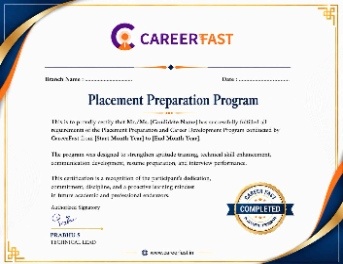
PCB Design Course in Adyar certification validates your skills and knowledge in designing printed circuit boards, especially in areas like schematic development, PCB layout, and circuit verification.
Yes, the PCB Design industry offers various certifications depending on the software and specialization. These certifications help professionals demonstrate expertise in areas like schematic design, PCB layout, circuit simulation, routing, and fabrication.
Certification does not guarantee employment. Practical experience and project exposure are often necessary. Strong technical knowledge and problem-solving abilities are essential.
Yes, you can pursue certifications in multiple tools (e.g., Altium Designer, KiCad, OrCAD). Knowledge of multiple tools improves your career opportunities.
Yes, some PCB Design certification exams are available online through approved assessment platforms. Candidates may complete examinations remotely, depending on the certification provider and its assessment requirements.
Yes, employers often prefer candidates with practical PCB Design experience. Internships and hands-on projects can improve employment prospects. Understanding electronic circuits and manufacturing processes provides an advantage.
Yes, a PCB Design Training Institute in Adyar program can be a valuable investment if you seek structured learning with practical industry applications.
Frequently Asked Questions
- Yes, PCB Design training offers both classroom and online learning options, providing flexibility based on your schedule and learning preferences.
- Typically, PCB Design course certification training lasts 4 to 8 weeks, depending on the modules covered and training format.
- Self-paced learning options may provide additional flexibility, allowing learners to progress according to their individual schedules.
- Placement assistance includes resume preparation, mock interviews, and opportunities to connect with recruiting companies.
- The placement team coordinates interview schedules and provides guidance based on each candidate's preparation and readiness.
- The institute provides a course completion certificate, which may not have government recognition but can support applications for electronics industry positions.
- Yes, PCB Design certification in Adyar includes practical industry-oriented projects covering circuit schematics, PCB layouts, routing, and manufacturing processes.
