) 3K+
3K+
Start Your Learning Journey Today
550+ Students Placed Every Month Be The Next!


Our Hiring Partners
Curriculum Designed By Experts
Expertly designed curriculum for future-ready professionals.
Industry Oriented Curriculum
An exhaustive curriculum designed by our industry experts which will help you to get placed in your dream IT company
-
30+ Case Studies & Projects
-
9+ Engaging Projects
-
10+ Years Of Experience
PCB Design Training Projects
Become a PCB Design Expert With Practical and Engaging Projects.
- Practice essential Tools
- Designed by Industry experts
- Get Real-world Experience
LED Blinker Circuit Board
Learn the basics of circuit design with a simple LED flasher using a 555 timer. Focus on schematic creation, component placement, and single-layer board design.
USB Power Supply Module
Design a PCB that converts USB 5V to 3.3V and 9V using voltage regulators. Practice working with through-hole components and DC power routing. Introduces power path design and decoupling capacitors.
Battery-Powered Mini Fan Controller
Build a fan controller circuit using transistors and resistors. Learn how to route signals, handle thermal pads, and place connectors.
Temperature Sensor with Display
Design a PCB that reads temperature and displays values using a 7-segment display. Incorporate analog-to-digital conversion and microcontroller interface.
Arduino Nano Based Relay Control Board
Create a PCB that allows Arduino Nano to control AC devices via relays. Practice mixed-signal routing and optocoupler isolation techniques.
Digital Voltmeter Circuit
Design a voltage measuring device with LCD output. Work on ADC interfacing and voltage divider design. Emphasis on signal accuracy, trace width, and grounding techniques.
ESP32 Wi-Fi Enabled Smart Switch
Design a PCB with Wi-Fi capability to control devices remotely. Implement SMD components, power management, and antenna layout. Learn complex routing, grounding, and signal shielding.
Multilayer PCB for Motor Driver Board
Create a compact, high-current motor driver board with a 4-layer PCB. Focus on heat dissipation, power trace optimization, and EMI control. Includes motor feedback routing.
Wearable Health Monitor
Design a small PCB that interfaces with biometric sensors and Bluetooth. Involves dense component placement and low-noise analog routing. Prioritize form factor, battery management, and data transmission
Career Support


Placement Assistance

Exclusive access to ACTE Job portal

Mock Interview Preparation

1 on 1 Career Mentoring Sessions

Career Oriented Sessions

Resume & LinkedIn Profile Building
Key Features

Practical Training

Global Certifications

Flexible Timing

Trainer Support

Study Material

Placement Support

Mock Interviews

Resume Building
Upcoming Batches
What's included

 Free Aptitude and
Technical Skills Training
Free Aptitude and
Technical Skills Training
- Learn basic maths and logical thinking to solve problems easily.
- Understand simple coding and technical concepts step by step.
- Get ready for exams and interviews with regular practice.

 Hands-On Projects
- Work on real-time projects to apply what you learn.
- Build mini apps and tools daily to enhance your coding skills.
- Gain practical experience just like in real jobs.

 AI Powered Self
Interview Practice Portal
AI Powered Self
Interview Practice Portal
- Practice interview questions with instant AI feedback.
- Improve your answers by speaking and reviewing them.
- Build confidence with real-time mock interview sessions.

 Interview Preparation
For Freshers
Interview Preparation
For Freshers
- Practice company-based interview questions.
- Take online assessment tests to crack interviews
- Practice confidently with real-world interview and project-based questions.
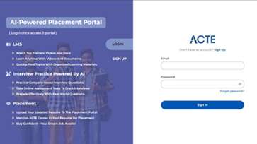
 LMS Online Learning
Platform
LMS Online Learning
Platform
- Explore expert trainer videos and documents to boost your learning.
- Study anytime with on-demand videos and detailed documents.
- Quickly find topics with organized learning materials.
- Learning strategies that are appropriate and tailored to your company's requirements.
- Live projects guided by instructors are a characteristic of the virtual learning environment.
- The curriculum includes of full-day lectures, practical exercises, and case studies.

PCB Design CourseOverview
PCB Design Training in Chennai – Programmer’s Potential Career Paths
Completing PCB Design Training in Chennai can open several exciting career opportunities in the electronics and embedded systems industries. Trainees can pursue roles such as PCB Design Engineer, Hardware Design Engineer, or Embedded Systems Developer. With industry-relevant skills, they can also work in R&D departments, manufacturing units, or become freelance circuit designers for global clients. As IoT and smart devices continue to grow, PCB professionals are increasingly in demand for designing compact, high-performance boards. Advanced learners can even transition into product development or technical consultancy roles.
What Are the Requirements for a PCB Design Course in Chennai?
- Basic Electronics Knowledge: A fundamental understanding of resistors, capacitors, ICs, and circuit behavior is essential.
- Computer Literacy: Familiarity with using Windows or Linux systems and installing software tools like KiCad, Eagle, or Altium Designer.
- Educational Background: Ideal for students pursuing or holding diplomas/degrees in ECE, EEE, Mechatronics, or related fields.
- Analytical Thinking: Problem-solving mindset and logical reasoning help in schematic design and troubleshooting.
- Interest in Hardware Design: A genuine interest in building electronic devices and understanding how physical circuits work is a big plus.
Reasons to Consider Enrolling in PCB Design Placement in Chennai
Enrolling in a PCB Design Placement program in Chennai offers more than just education—it provides a gateway to a stable and growing career. With Chennai being a hub for electronics and manufacturing companies, trained professionals have access to numerous job opportunities. The placement support offered by institutes includes resume building, mock interviews, and connections with hiring companies. Real-time projects enhance portfolio strength and industry credibility. Students receive exposure to both software tools and fabrication techniques. Ultimately, this training can fast-track your career into core electronics roles.
Techniques and Trends in PCB Design Training in Chennai
- High-Speed PCB Design Techniques: Learn how to design boards that support high-frequency signals with minimal noise and signal loss.
- Thermal Management in PCB Layout: Training includes designing heat sinks, thermal vias, and power planes to manage device temperature.
- Design for Manufacturability (DFM): Emphasis on designing PCBs that are optimized for large-scale production and easier testing.
- Flexible and Rigid-Flex PCB Design: Explore the latest in wearable and foldable electronics through advanced PCB materials and structures.
- EMI/EMC Considerations: Understand how to minimize electromagnetic interference and comply with global standards.
The Most Recent PCB Design Training Tools
Modern PCB Design training in Chennai uses state-of-the-art tools such as Altium Designer, KiCad, Eagle, and OrCAD. These platforms support advanced features like auto-routing, 3D modeling, signal integrity checks, and multilayer design. Training also includes simulation tools like LTspice or Proteus to validate circuits before physical prototyping. Real-time collaboration tools and cloud storage features help teams design remotely. Learners gain hands-on experience with fabrication file generation (Gerber), BOM creation, and online PCB ordering. These tools ensure students are job-ready for current and future design environments.
Career Opportunities After PCB Design Training
PCB Design Engineer
Design and develop PCB layouts ensuring signal integrity and manufacturability for electronics products. Collaborate with hardware engineers to optimize designs. Also responsible for reviewing design specifications and implementing improvements.
Electronics Design Engineer
Create electronic circuit schematics and PCB layouts, test prototypes, and troubleshoot design issues for consumer and industrial electronics. Participate in cross-functional teams to support product development from concept through production.
Layout Designer
Focus on the physical placement and routing of PCB components, adhering to design rules and manufacturing constraints. Ensure compliance with industry standards and optimize layouts for high-speed and high-frequency designs.
Hardware Engineer
Work on hardware architecture, PCB design, and integration of circuits, ensuring functionality and reliability. Conduct hardware validation and verification testing to meet product requirements.
Manufacturing Engineer
Manage PCB fabrication processes, quality control, and testing procedures to ensure products meet industry standards. Coordinate with suppliers and production teams to streamline manufacturing and reduce defects.
Test Engineer
Develop and execute test plans for PCBs, identify faults, and ensure product performance meets specifications. Analyze test data and provide feedback to design teams to improve product reliability.
Skill to Master
Circuit schematic creation
PCB layout and routing techniques
Signal integrity and noise reduction
Design rule checking
Component library management
Multi-layer board design
Gerber file generation
BOM preparation
EMC mitigation strategies
Thermal management of PCBs
Troubleshooting and debugging
PCB fabrication
Tools to Master
Altium Designer
Eagle PCB
KiCad
Mentor Graphics PADS
Proteus
DipTrace
CircuitMaker
EasyEDA
DesignSpark PCB
Target 3001
Assembly process knowledge
Pulsonix
Learn from certified professionals who are currently working.

Training by
Divya , having 9 years of experience
Specialized in: Layout Designer,Manufacturing Engineer and PCB Design Engineer.
Note: Divya is recognized for her deep knowledge of PCB layout techniques and her ability to bridge the gap between theory and practical electronics design.
Premium Training at Best Price
Affordable, Quality Training for Freshers to Launch IT Careers & Land Top Placements.
What Makes ACTE Training Different?
Feature
ACTE Technologies
Other Institutes
Affordable Fees
Competitive Pricing With Flexible Payment Options.
Higher Fees With Limited Payment Options.
Industry Experts
Well Experienced Trainer From a Relevant Field With Practical Training
Theoretical Class With Limited Practical
Updated Syllabus
Updated and Industry-relevant Course Curriculum With Hands-on Learning.
Outdated Curriculum With Limited Practical Training.
Hands-on projects
Real-world Projects With Live Case Studies and Collaboration With Companies.
Basic Projects With Limited Real-world Application.
Certification
Industry-recognized Certifications With Global Validity.
Basic Certifications With Limited Recognition.
Placement Support
Strong Placement Support With Tie-ups With Top Companies and Mock Interviews.
Basic Placement Support
Industry Partnerships
Strong Ties With Top Tech Companies for Internships and Placements
No Partnerships, Limited Opportunities
Batch Size
Small Batch Sizes for Personalized Attention.
Large Batch Sizes With Limited Individual Focus.
LMS Features
Lifetime Access Course video Materials in LMS, Online Interview Practice, upload resumes in Placement Portal.
No LMS Features or Perks.
Training Support
Dedicated Mentors, 24/7 Doubt Resolution, and Personalized Guidance.
Limited Mentor Support and No After-hours Assistance.
We are proud to have participated in more than 40,000 career transfers globally.

PCB Design Certification

Certification improves your credibility and skillset and guarantee a job. Employers value experience, portfolio projects, and problem-solving skills alongside certification.
Absolutely! Gaining certifications from different tools or specialized areas (e.g., high-speed PCB design, embedded PCB) can broaden your expertise and enhance your career prospects.
Many institutes and certification bodies offer online exams or remote proctored tests, especially after COVID-19. Check with the specific certification provider for their exam mode.
While entry-level roles may accept freshers with strong training and projects, real-world experience significantly boosts employability and confidence. Internships or practical training help bridge this gap.
Yes, ACTE certifications are well-recognized, with focused curriculum and experienced instructors. They often provide hands-on training and placement support, making them valuable for career starters.
Frequently Asked Questions
- You will learn how to create schematic diagrams, design PCB layouts using software tools, understand component placement, routing techniques, and manufacturing processes.
- The course covers single-layer to multilayer PCB designs, signal integrity, thermal management, and hands-on project experience to build practical skills.
- No prior experience is necessary.
- The course starts with basic electronics and PCB design fundamentals, making it suitable for beginners as well as those looking to upgrade their skills.
- ACTE helps students build portfolios by guiding them through multiple real-world projects, offering mentorship, and providing access to design resources.
- Yes, you will receive a verified certificate upon successful completion of the course, which can be shared with potential employers to showcase your PCB design skills.
- Absolutely! ACTE organizes demo days, project exhibitions, and online showcases where students can present their PCB designs to industry experts and recruiters, increasing their chances of getting noticed.